
会長の略歴
弊社会長の川人祥二は、静岡大学教授として長年イメージセンサの研究、開発に携わってまいりました、そこで得た多くの知識、経験、特許を活かし企業様からのご要望に合ったイメージセンサの共同研究、開発も行っております。
SUiCTEの「役割」は、これらの開発プロジェクトを画素、アナログ/デジタル回路、システム、評価・解析など経験豊富な自社エンジニアと共に事業化を行ってまいります。尚、静岡大学とは共同研究開発協定を締結しております。
Sensor Technologies
https://www.ite.or.jp/contents/venture/1807venture.pdf 2018 ITE
https://ieeexplore.ieee.org/document/8310198 2018 ISSCC
Technologies for Image Sensor Ⅰ
Technologies for Image Sensor Ⅱ
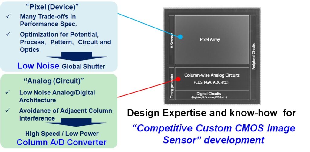
1) Pixel Design
★ Optimization by considering many Trade-offs
★ Global Shutter
★ Time of Flight
→Customize Pixel with Foundry
2) Analog Design
★ Low noise Amplifier
★ High Speed ADC(A/D Converter) = Cyclic ADC
Cf. Sony/OVT : Single Slope ADC
Aptina : SAR ADC
Technologies for Image Sensor Ⅲ
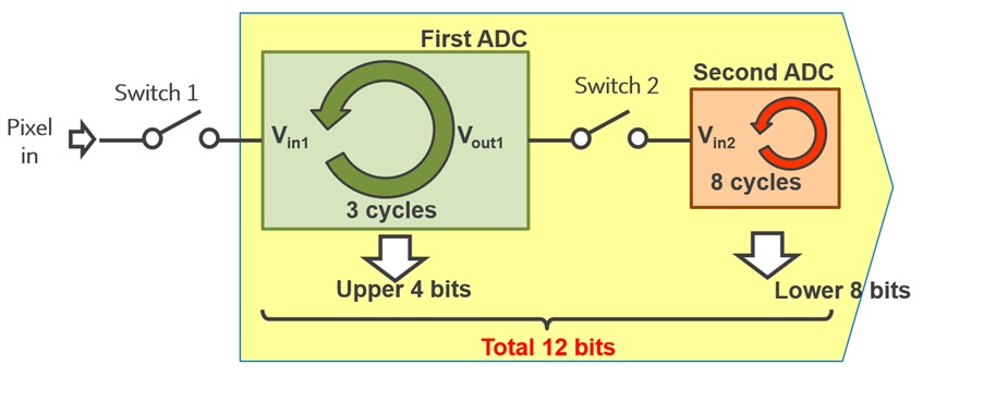
2-stage Column Parallel Cyclic A/D Converter
・Optimize the topology of the basic 2-stage Cyclic A/D Converter
・Brushed up the design for circuit and layout
High Speed (1MS/s)
High Bit Resolution (12bit)
Low Power (<120uW/ADC)
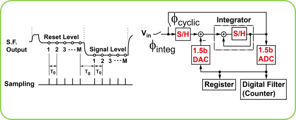
Correlated-Multiple-Sampling (CMS) 16b A/D Converter
◆Our CMS-based cyclic ADC realizes ultra-low-noise wide-dynamic-range CMOS imagers for High-End DSC, Security Camera, Remote Sensing, etc.
Ultra Low Noise (0.3e-*)
High Bit Resolution (16bit)
Wide Dynamic Range (>90dB)
High Conversion Gain Pixel is used.
Technical Papers for Image Sensor
◆ 2017.02. ISSCC
“A 0.44e-rms Read-Noise 32fps 0.5Mpixel High-Sensitivity RG-Less- Pixel CMOS Image Sensor Using Bootstrapping Reset”
◆ 2016.02. ISSCC
“A 1.1μm 33Mpixel 240fps 3D-Stacked CMOS Image Sensor with 3-Stage Cyclic-Based Analog-to-Digital Converters”
◆ 2012.02. ISSCC
“A 33Mpixel 120fps CMOS Image Sensor Using 12b Column-Parallel Pipelined Cyclic ADCs”
◆ 2011.06. IISW
“A High Speed Low-Noise CIS with 12b 2-stage Pipeline Cyclic ADCs”
◆ 2011.06. IISW
“A 33Mpixel, 120fps CMOS Image Sensor for UDTV Application with Two-stage Column- Parallel Cyclic ADCs”
Technologies for Time of Flight Sensor I
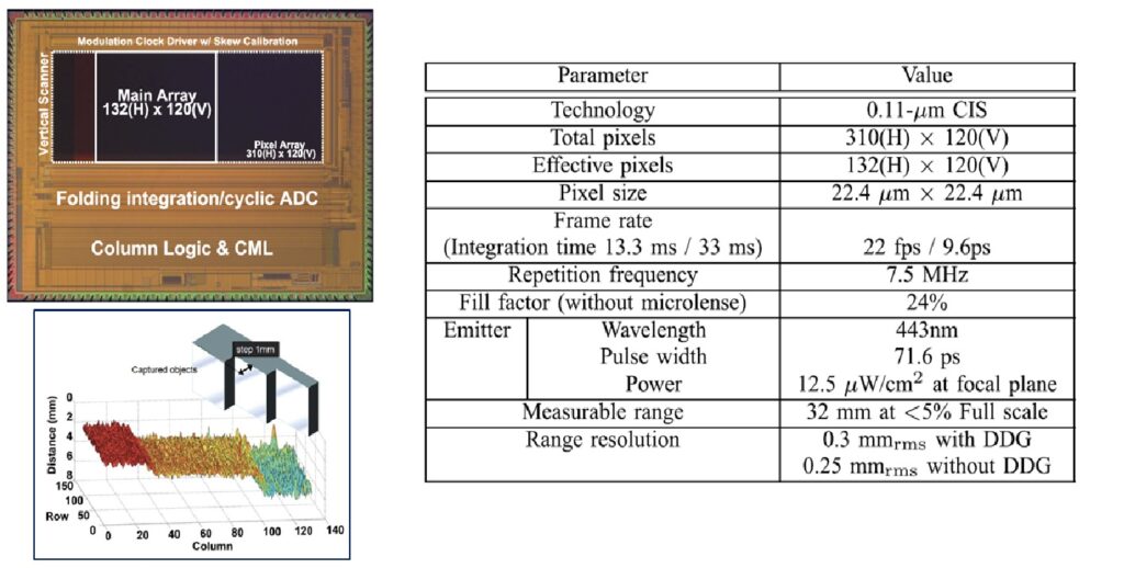
Technical Papers for Time of Flight Sensor
2015.05. J-EDS
“A Time-of-Flight Range Image Sensor with Background Cancelling Lock-in Pixels Based on Lateral Electric Field Charge Modulation”,
2016.01. Trans. on ED
“A Submillimeter Range Resolution Time-of-Flight Range Imager With Column-Wise Skew Calibration”
2016.01. Trans. on ED
“A 10 ps Time-Resolution CMOS Image Sensor With Two-Tap True-CDS Lock-In Pixels for Fluorescence Lifetime Imaging”
2014.08. Opt. Express
“Indirect time-of-flight measurement technique with impulse photocurrent response for sub- millimeter range resolved imaging”
2016.02. Opt. Express
“Single-event transient imaging with an ultra-high-speed temporally compressive multi-aperture CMOS image sensor”
Evaluation and Analysis Technologies
We can provide your pixels characterization data as well as haracterization environment and method and also FA data and method w/ OBRICH, SEM and TEM based on our rich experience.
Design Experiences on Large field image sensor
- Our strong point is Large format image sensor developments w/ special purpose.
- We have developed more than 15 large field image sensors w/ stitching on 0.11um CIS process in some foundry
- We have an Foundry expert who worked for some foundry for 15 year at technical support for Japanese customers on various processes include CIS processes.
◆Flexible image sensor design is available on a Large field image sensor
- Consideration for IR drop on bus lines.
- Keep clock simultaneity on a chip everywhere.
- Adjust many of High speed outputs data timing.
- Control Pixels behavior at stitching area.
- Ideas and experiences for large-field chip cost down and yield improvement.
- Test program development is available by ourselves, we can use Shizuoka univ. testers for image sensor.
- Failure analysis and short and log term reliability testing are also available.